CD4011 (Quad 2-Input NAND Gate)
The CD4011 is a Quad 2-input NAND gate integrated circuit (IC) from the 4000 series of CMOS logic ICs. It contains four independent 2-input NAND gates in a single 14-pin package. The IC is commonly used in various digital applications for implementing basic logic functions such as AND, OR, and NOT by combining NAND gates in different configurations.
Key Features of CD4011:
- Function:
- The CD4011 contains four 2-input NAND gates. A NAND gate outputs a low (0) only when both inputs are high (1). In all other cases (if either or both inputs are low), the output will be high (1).
- The truth table for a 2-input NAND gate is as follows:
A B Output (A NAND B) 0 0 1 0 1 1 1 0 1 1 1 0
- Voltage Range:
- The CD4011 operates over a wide voltage range, typically from 3V to 15V, making it compatible with both TTL (Transistor-Transistor Logic) and CMOS (Complementary Metal-Oxide-Semiconductor) logic systems.
- Package Type:
- The CD4011 is available in various package types, with the most common being the DIP-14 (Dual In-Line Package) and SOIC (Surface-Mount) packages.
- Low Power Consumption:
- As a CMOS IC, the CD4011 features low power consumption. It consumes very little current, making it ideal for battery-operated systems and other low-power applications.
- Noise Immunity:
- The CMOS design provides high noise immunity, making the CD4011 reliable even in environments with significant electrical noise.
- High Output Drive Capability:
- The CD4011 can drive standard CMOS outputs and can interface with other logic circuits or peripheral devices directly.
- Temperature Range:
- The typical operating temperature range for the CD4011 is -55°C to +125°C, which allows it to work in both industrial and consumer-grade applications.
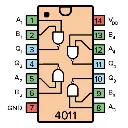
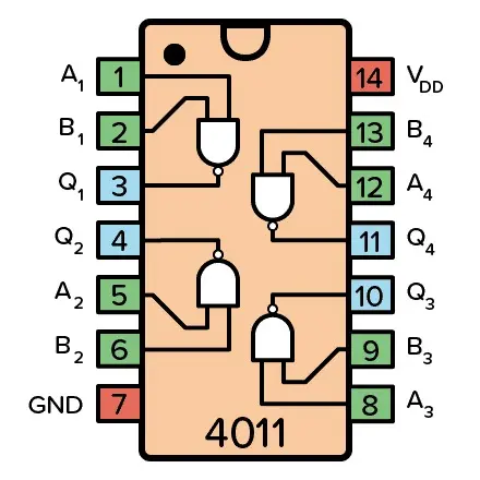
Pin Configuration of CD4011 (DIP-14 Package):
| Pin No. | Pin Name | Description |
|---|---|---|
| 1 | A1 | Input 1 of NAND Gate 1 |
| 2 | B1 | Input 2 of NAND Gate 1 |
| 3 | Y1 | Output of NAND Gate 1 (A1 NAND B1) |
| 4 | A2 | Input 1 of NAND Gate 2 |
| 5 | B2 | Input 2 of NAND Gate 2 |
| 6 | Y2 | Output of NAND Gate 2 (A2 NAND B2) |
| 7 | GND | Ground |
| 8 | A3 | Input 1 of NAND Gate 3 |
| 9 | B3 | Input 2 of NAND Gate 3 |
| 10 | Y3 | Output of NAND Gate 3 (A3 NAND B3) |
| 11 | A4 | Input 1 of NAND Gate 4 |
| 12 | B4 | Input 2 of NAND Gate 4 |
| 13 | Y4 | Output of NAND Gate 4 (A4 NAND B4) |
| 14 | Vcc | Power supply (typically 5V or 12V) |
Applications of the CD4011:
- Digital Logic Design:
- The NAND gate is a universal gate, meaning any logical function can be implemented using only NAND gates. The CD4011 can be used in various combinational logic circuits, including creating AND, OR, NOT, and more complex logic operations by combining NAND gates.
- Arithmetic Circuits:
- The NAND gate is used in binary adders and other arithmetic circuits. In particular, half adders and full adders are commonly built using NAND gates.
- Control Systems:
- The CD4011 can be used in control systems where multiple conditions need to be checked simultaneously. For example, in digital controllers, multiple inputs can be processed with NAND gates to make logical decisions.
- Flip-Flops and Memory Circuits:
- SR Latches and flip-flops (like D flip-flops) can be implemented using NAND gates, allowing the CD4011 to be used in memory storage, registers, and synchronization circuits.
- Pulse Generation:
- NAND gates can be used to generate pulses or clock signals. The IC can be used in timing circuits, where specific delays or pulse widths are required.
- Signal Processing:
- The CD4011 can be used in signal processing applications such as creating pulse width modulation (PWM) signals, oscillators, and timers.
- Frequency Dividers:
- The IC is useful for implementing frequency dividers or other digital frequency manipulation applications. By combining the NAND gates, you can create circuits that divide input frequencies or control digital clocking.
- Logic Gates for LED Drivers:
- The CD4011 can be used to drive LED displays or LED arrays where simple logic needs to be performed to control the LEDs.
Advantages of the CD4011:
- Low Power Consumption:
- As a CMOS IC, the CD4011 has low power consumption, which is beneficial in battery-operated or energy-efficient designs.
- Wide Voltage Range:
- The CD4011 operates over a broad voltage range (3V to 15V), which allows for flexibility in design and makes it compatible with different logic families like TTL and CMOS.
- Four Gates in One Package:
- The CD4011 contains four independent NAND gates in a single package, which reduces the number of ICs required in a design, making it more compact and cost-effective.
- Versatility:
- The NAND gate is a universal logic gate, meaning it can be used to implement any other basic logic gate (AND, OR, NOT). This makes the CD4011 versatile for a wide range of logic applications.
- High Noise Immunity:
- The CMOS technology provides excellent noise immunity, which makes the CD4011 stable and reliable in environments with electrical noise.